Business challenges
- Integration and verifcation of highly complex AI architecture
- Create next-generation ultra-performance AI NPU chiplets
ETRI’s AI NPU Development History
The Electronics and Telecommunications Research Institute (ETRI) is a government research institute focuses on IT and semiconductor components. In 2019, the AI NPU processor design group at ETRI’s National AI Research Institute developed the frst Korean AI processor, the AB9. An FP16 16-bit floating-point artifcial neural network computing processor, the AB9 has been successfully adopted by several commercial companies for their AI computing servers.
Coming off that success, the AI NPU processor design team sought to push the boundaries of AI even further by employing a chiplet-based design strategy to create their next-generation of AI processors – the ABS1 neural processing unit (NPU). ETRI wanted to take advantage of 3D IC packaging technology’s capability to dramatically increase bandwidth and performance while reducing the power and cost of their highly-complex, high-performance ASIC designs.
ETRI’s drive to innovation operates within a larger context in which the semiconductor industry faces a considerable technology inflection point as higher cost, lower yield, and reticle size limitations compel the demand for viable alternatives to traditional monolithic system-on-chip (SoC) architectures. This is driving an emerging trend to disaggregate device functions into solid, fabricated IP blocks implemented at the appropriate process node and technology, otherwise known as chiplets.
Multiple chiplets, memory, and an optional, custom ASIC device can be mounted and interconnected into a single package using high-speed, high-bandwidth chiplet-to-chiplet interfaces, such as those using the Bunch of Wires (BoW) and Universal Chiplet Interconnect Express (UCIe) specifcations. The resulting 3D IC heterogeneously integrated assembly can deliver greater performance at a reduced cost and higher yield, with only a slightly larger footprint
than a traditional monolithic SoC.
 3D IC heterogeneously integrated assembly
These chiplet architectures provide the increased compute power, memory access, and storage that ETRI’s AI processors require. Employing this truly groundbreaking chiplet technology, ETRI is equipped to create next-generation, ultra-performance NPUs.
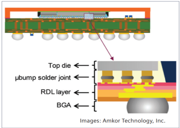
ETRI also wanted the high-speed design to boast advanced energy efciency and higher AI performance. To achieve these goals, the ABS1 integrates two AI NPU chiplets with eight HBM3 memory stacks. Ten of these dies are integrated on top of a large-scale redistribution-layer (RDL) interposer. The result will be the frst petaflops AI processor that has a very high energy efciency.
Amkor Korea utilized XPD for its excellent design capacity and performance, which they needed to handle their high-density advanced package designs, such as the RDL interposer. Further, for the design of the RDL interposer itself, XPD contains special functionalities that reduce design cycle times
Amkor had originally adopted XPD for their Silicon Wafer Integrated Fan-out Technology (SWIFT®), which enables the creation of advanced 3D structures, such as the RDL interposers and advanced package designs.
“ Siemens IC packaging design tools helped us provide a fast and highquality design service to our customers even with large body and chiplet package structures.”
JaeBeom Shim
Package Design Manager – Amkor Korea
Other features that XPD had in its favor were its “physical reuse circuit” function, which plays an especially important role in reducing total design cycle time, and XPD’s true GDS direct-export functionality. Its high-performance dynamic plane shapes capability was a big part of why they chose XPD for RDL interposer and large size package substrate design.
As well, Amkor has a great deal of experience using xSI for bump connection visualization and optimization during multi-die integration. xSI has proven to show superior design capacity even when dealing with bump counts in the hundreds of thousands.
xSI is packed with features that enable Amkor to integrate 3DSTACK level design structures for both the RDL interposer and the package substrate. xSI can handily perform the bump connection optimizations required to achieve a better quality RDL interposer design, which indeed was successfully done by xSI on the interposer. Amkor has been successfully running Calibre 3DSTACK verifcation for high-density advanced package designs, so they knew it was a good choice for ETRI’s AI NPU processor project.
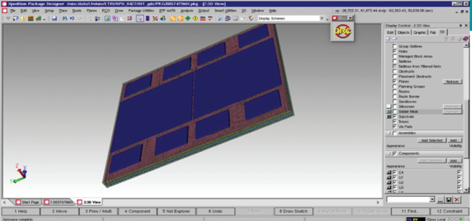 The ABS1 NPU being designed in Xpedition Package Designer by the Amkor advanced IC packaging design team (source: Amkor Technology)
ETRI initially focused on constructing a seamless VLSI CAD flow for advanced packaging, using xSI to describe the top-level chiplet architecture of the ABS1 NPU composed of multiple dies, chiplets, and HBM3 stacks. By providing this description of the top chiplet architecture, xSI then allowed them to seamlessly move on to the architecture simulation tool environment, Xpedition Package Designer (xPD), for interposer and package substrate design.
When they started RDL interposer design, netlist information about the NPU die and the HBM die was only in Verilog. So they needed Siemens to provide tools that could visualize bump-to-bump connections and micro-bumps-to-C4-bumps, including the package BGA. Indeed, xSI is capable of not only connection visualization but also optimizing connections. ETRI was very satisfed with how xSI performed these functions.
Amkor also needed to verify connectivitychecks of the multi-die architecture, the RDL interposer, and the package substrate in ETRI’s hierarchical, high-density advanced packages. All these checks were successfully performed using the xSI-Calibre 3DSTACK verifcation flow,
which generated source level netlist and connectivity-checks between the multidie structures, the interposer, and the package substrate.
“Amkor has successfully provided package designs from RDL interposer to substrate.We also verifed the connectivity and performed DFM with xSI and Calibre 3DSTACK. Siemens IC packaging design tools helpedus provide a fast and high-quality design service to our customers even with large package and chiplet package tructures,”
JaeBeom Shim, the Amkor package design manager in Korea reports.
At the end of the design work, ETRI successfully completed 3DSTACK verifcation sign-off for both the interposer and the 3D IC package.
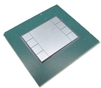 The final ABS1 device is the first petaflops AI processor with very high energy efficiency (source: Amkor Technology)
Read more:
- Leonardo optimizes electronic systems with Xpedition, HyperLynx, and Valor
- Nobo Auto optimizes PCB design with Xpedition & HyperLynx
- Calibre Auto-Waivers