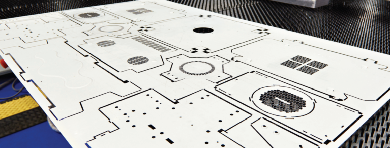
The semiconductor industry is on track to being worth $1 trillion by 2030. While accelerating demand will help semiconductors reach impressive gains, many chip makers may be held back by the costs of fabrication (also known as a fab) construction and semiconductor design. Already, building a fab costs about $19 billion and the design of each chip is a $1 billion investment on average.
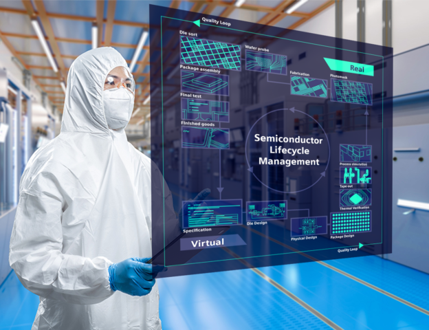
More and more hardware products are beginning to rely significantly on software, software defined products will become increasingly central to the evolution of the semiconductor industry. Part of creating improved environments to better fabricate custom parts for SDPs is making sure that the process remains affordable. To combat production costs that are likely to rise, semiconductor companies should lean into digitalization and leverage the comprehensive digital twin for both the semiconductor design and fabrication.
Taking advantage of virtual space
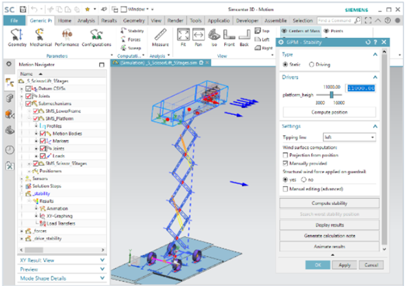
The comprehensive and physics-based Digital Twin (cDT) addresses the challenge of how to weave together the disparate engineering and process groups needed to design and create tomorrow’s SW-enabled semiconductor. To enable all these players to interact early and often, the cDT incorporates mechanical, electronic and electrical software and manufacturing to fully capture today’s smart products and processes.
Specifically, the cDT merges the real and digital worlds by creating a set of consistent digital models representing different facets of the design that can be used throughout the entire product and production lifecycle and the supply chain. Now it is possible to do more virtually before committing to expensive prototypes or physically commissioning a fab. The result is higher quality products while meeting aggressive cost, timeline and sustainability goals
In design, this ‘shift-left’ provides a physics-based virtual environment for all the engineering teams to interact and create, simulate, and improve product designs. Design iterations in the virtual world happen quickly and consume few resources outside of the engineer’s brain power, enabling them to explore a broader design space. Then in production, it empowers companies to virtually evaluate and optimize production lines, commission machines, and examine entire factories or networks of factories to improve production speed, efficiency, and sustainability. It can analyze and act on real data from the fab and then use that wealth of data for AI metrics analysis.
The comprehensive digital twin for the semiconductor ecosystem helps businesses manage the complexities of integrating software and hardware teams as well as mechanical and production requirements while bolstering efficiency. Benefits of the digital twin include:
- Faster new product introductions: virtualizing the design phase speeds up prototype creation, which will become even more important as the quest to pursue “More than Moore” normalizes advanced packaging
- Faster path to higher yields: simulating the production process makes enhancing IC quality easier, enabling workers to enact changes dynamically on the shop floor to quickly achieve higher yields for greater profitability
- Traceability and zero defects: it is now possible to update the digital twin of both the product and production in tandem with their real-world counterparts, enabling manufacturers to diagnose issues and detect anomalies before they happen in the pursuit of zero defects
- Dynamic planning and scheduling: since the digital twin provides an adaptive comparison between the physical and digital counterparts, it can detect disturbances within systems and trigger rescheduling in a timely manner
Simplifying for better gains
Creating next-generation semiconductors is expensive. Yet, chip manufacturers must continue to develop and fabricate new designs that require ever-more advanced fabrication technology to efficiently create the software-defined semiconductor for tomorrow’s software-defined products. To handle the changing landscape, businesses within the semiconductor industry will need to rely on the comprehensive digital twin.
Businesses can leverage the cDT to virtualize the entire semiconductor process design for the SW enabled product, enabling them to simulate everything from initial design concepts to manufacturing processes and final product integration, which dramatically reduces development cycles and improves outcomes. Integrating processes and using dating to its full potential will ensure that the semiconductor market reaches the $1 trillion milestone.
(Source: Siemens)
Read more:
- Arm finds success with Siemens Aprisa place-and-route
- Top 6 reasons to choose IC design solutions from Siemens EDA