
When multiple dies are vertically integrated in a 3D IC architecture, thermal management can no longer be treated as a late-stage design issue. High power density, close proximity between heat sources, and increasingly complex heat dissipation paths can create hotspots even when the overall power consumption remains within acceptable limits.
Thermal analysis should therefore begin during the architectural planning stage and extend from the die and package level through to the cooling system. This approach allows engineers to compare design options early, identify potential risks, and minimize costly modifications as the design approaches signoff.
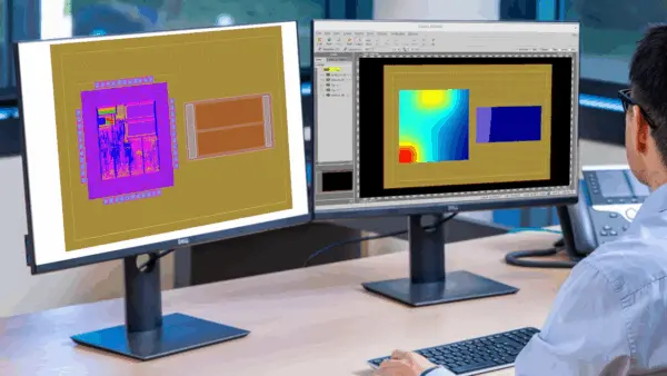
Why is thermal management more challenging in 3D IC design?
Unlike conventional 2D ICs, dies in a 3D IC are stacked within a much smaller volume. This increases local heat density and allows heat generated by one die to directly affect neighboring dies.
High power density and localized hotspots
Logic dies, memory, and other functional blocks do not consume power uniformly. When several high-power regions are located close together, hotspots can develop even if the total system power remains within its specified limits.
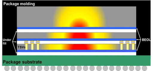
More complex heat dissipation paths
Heat generated by a die may need to travel through silicon, bonding layers, interface materials, and multiple package components before reaching the heat sink. Each interface introduces additional thermal resistance and can become a bottleneck in the heat dissipation path.
Thermal interaction between dies
Even a relatively low-power die can experience elevated temperatures because of heat generated by an adjacent die. Evaluating each die independently may therefore fail to represent the actual operating conditions of the complete stack.
Key factors that determine heat dissipation in 3D ICs
- Thermal performance in a 3D IC depends on a combination of material properties, package architecture, die placement, and the cooling solution.
- TSVs (Through-Silicon Vias) not only provide electrical connectivity but also influence heat flow through the stack. Their thermal impact depends on material composition, density, and location relative to heat sources, so TSVs should be evaluated as part of the overall thermal model.
- Thermal Interface Materials (TIMs) and bonding layers also play an important role. High thermal resistance at these interfaces can become a bottleneck, meaning that optimizing the silicon or heat sink alone may not deliver the expected improvement.
- Package architecture and the cooling system determine how heat is removed from the die stack. Thermal optimization should therefore be performed at the system level rather than by optimizing individual components in isolation.
When should thermal modeling begin in a 3D IC project?
Start at the system architecture stage
During the early stages of development, simplified thermal models can be used to compare stacking orders, die placement, power distribution, and package configurations. At this stage, the objective is not signoff-level accuracy, but to quickly identify and eliminate design options with high thermal risk.
As the design matures, the model can be refined with more detailed geometry, accurate material properties, and realistic boundary conditions. This provides continuity from architectural exploration through final design verification.
Combine steady-state and transient thermal analysis
| Method | Purpose | Typical application |
|---|---|---|
| Steady-state | Determine temperature distribution once the system reaches thermal equilibrium | Compare stack configurations, package designs, and heat dissipation under sustained loads |
| Transient | Track temperature changes over time | Evaluate dynamic workloads, switching activity, and different operating cycles |
The two approaches complement each other. Steady-state analysis helps determine thermal limits under stable operating conditions, while transient analysis shows how the system responds as workloads and power levels change over time.
Maintain consistent data from chip to system
Information such as power consumption, die placement, material properties, and cooling conditions must remain synchronized across design teams. Chip–package co-design allows architectural changes to be reflected consistently throughout analysis and verification.
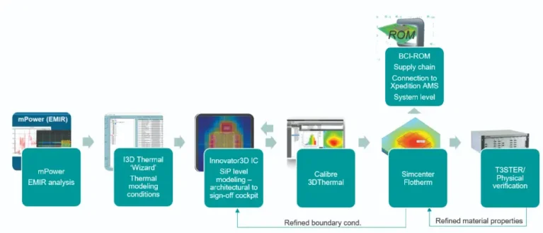
Thermal optimization strategies for 3D IC design
- Optimize die placement and stacking order: Placing high-power dies closer to the heat dissipation path can help reduce peak temperatures. However, this decision must also be balanced against electrical connectivity, routing, and packaging requirements.
- Optimize thermal interfaces and materials: TIMs, bonding layers, and material interfaces should be modeled using realistic data. Early assumptions should be progressively updated as the design approaches signoff.
- Use multiphysics analysis rather than thermal analysis alone: A change that improves thermal performance may affect electrical performance, mechanical stress, or manufacturability. Design options should therefore be evaluated across thermal, electrical, and mechanical domains.
Frequently asked questions about thermal management in 3D ICs
| Question | Answer |
|---|---|
| When should thermal analysis begin in a 3D IC project? |
Thermal analysis should begin during architectural planning, while stacking order, die placement, and power distribution can still be changed relatively easily. |
| Do TSVs always improve heat dissipation? |
No. The thermal impact of TSVs depends on their material composition, density, placement, and the overall structure of the design. |
| Does every 3D IC require advanced cooling technologies? |
Not necessarily. Many thermal challenges can first be addressed through architecture optimization, stack configuration, and thermal interface improvements before more complex cooling technologies are required. |
| What is one of the most common mistakes in 3D IC thermal management? |
A common mistake is waiting until the design is nearly complete before performing detailed thermal analysis. At that stage, architectural changes become more difficult and significantly more expensive to implement. |
Conclusion
Effective thermal management in 3D ICs should begin at the architectural stage and continue throughout the entire design process. Combining thermal modeling, package data, and multiphysics analysis enables engineers to identify hotspots earlier, evaluate design alternatives, and reduce risk as the design approaches signoff.
Are you exploring thermal analysis and 3D IC design solutions?
Contact Vietbay to learn more about suitable Siemens EDA solutions for your project.