For the past few decades, the semiconductor industry has been ahead of the curve when it comes to digitalization. Even still, there are still many opportunities for further digital transformation within the industry as both design costs and complexity continue to increase. Designing a chip is a nearly $1 billion investment. As well, modern semiconductor devices contain billions of transistors and building them requires extreme precision due to their microscopic scale.

Additionally, with the increased demand for software-defined products (SDPs), engineers now have to design hardware with software in mind all while collaborating with peers across several disciplines. This intra-disciplinary collaboration is especially intricate as complex methodologies and tools are needed to guarantee successful cooperation.
During an enlightening podcast discussion with Dale Tutt, industry strategy leader at Siemens, Aerospace Executive, Engineering and Program Leadership, Michael Munsey, VP of Siemens Semiconductor Industry, outlined how digital tools can help chipmakers simplify and optimize their processes as challenges in semiconductor intensify.
Easing collaboration with the digital twin
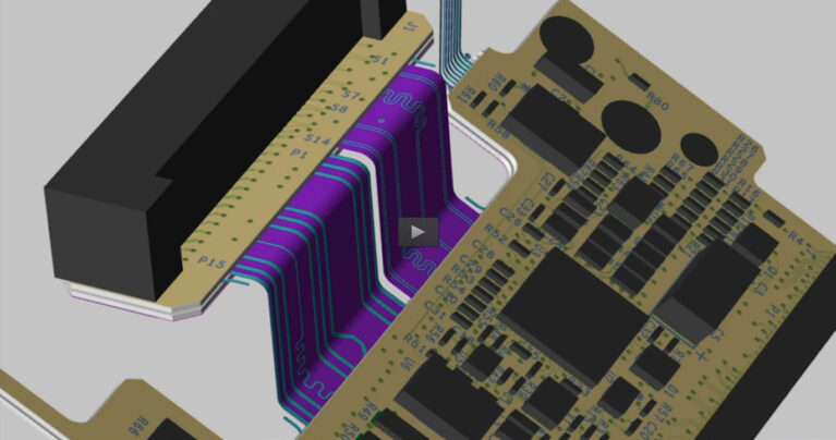
Chips themselves have become especially elaborate to fab. Many SDPs require high-performing, energy efficient chips that can fit in compact devices like cellphones. To adjust to these demands, many chipmakers deploy advanced packaging techniques which aid in lowering energy consumption and heat accumulation while enhancing the speed and performance of the chip.
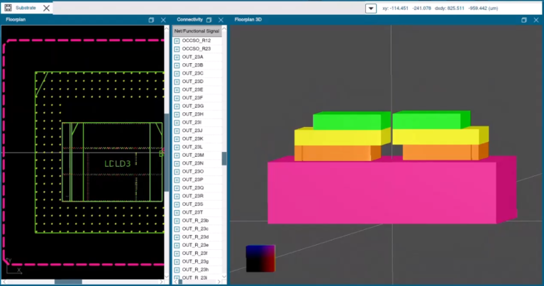
Designing and fabbing these chips requires digital verification to manage interactions and potential failure modes. A comprehensive digital twin (cDT) is essential for validating and verifying performance as the process to design and manufacture chips becomes more elaborate. Working as a single source of truth, the cDT integrates mechanical, electronic, and software components into a single virtual environment, allowing for seamless interaction and collaboration among different engineering teams.
As well, simulating the chip early in the design phase can help teams spot potential issues before building physical prototypes. Utilizing the detailed, physics-based simulations of the cDT, manufacturers can accurately recreate the chip’s real-world behavior, improving the reliability of tests. The cDT’s accurate simulations support a wide range of tests, helping teams thoroughly verify all aspects of the design.
Gaining insights with AI
The cDT further simplifies organizational processes by capturing data throughout the entire design and verification process. Manufacturers can then use this data to gain insights into performance and optimize the product lifecycle. Leveraging AI, teams can analyze verification data, optimize test coverage, and generate new test cases, making the verification process more efficient and effective.
AI has a wealth of capabilities that can facilitate multi-team operations and optimize the complex design process of semiconductors. With AI, chipmakers can see benefits such as:
- Improved decision-making through capturing and analyzing data from design and verification
- Augmented processes and quicker design periods through extending digital models into the manufacturing world
- Optimized product development through automating system-level analysis
Furthermore, AI can learn from the data it has collected, enabling it to continuously learn and improve its strategies. This continuous learning ensures that the verification process becomes more efficient and effective with each iteration, potentially laying the groundwork for greater automation in the future. Taking advantage of AI helps to streamline the verification process, making it more capable of handling the increasing complexity of modern semiconductor designs.
Create intricate chips through simplified design
The semiconductor industry is relatively mature in its digitalization journey. Even still, further digitalization can address new and even upcoming design and manufacturing challenges. Fabbing chips is an elaborate process and it stands to become even more complex as businesses increasingly introduce more SDPs and AI chips become more prevalent.
Harnessing the power the power of the cDT and AI can help manage the complex processes needed to design in-demand chips. With the simulation capabilities of the digital twin, chipmakers can declutter the verification process while facilitating cross-team collaboration. As well, AI tools can help organizations use data to their advantage while increasing automation capabilities. When used in conjunction with the cDT, manufacturers may see new levels of optimization and efficiency.
(Source: Siemens)
Read more:
- Smarter, Faster AI Chip Design with Siemens’ 3D IC Packaging Technology at ETRI and Amkor
- How AI is accelerating semiconductor testing
- How AI will enable DevOps for hardware