Chiplets are revolutionizing the semiconductor industry, enabling unprecedented levels of integration, performance, and flexibility. By breaking complex designs into smaller, specialized “chiplets” designers can overcome manufacturing limitations, mix and match technologies, and accelerate time-to-market.
But there’s a critical hurdle that often gets overlooked: how do you ensure that these disparate chiplet, often from different foundries and process nodes, will work together flawlessly when integrated into an advanced package?
If you’re a package designer, a system-level architect, or an IC design engineer working on chiplet-based products, you know the challenge. Traditional IC verification methods, designed for monolithic chips, simply aren’t up to the task.
The verification gap: Why traditional methods fall short
The core problem lies in a significant “verification gap” in IC-package co-design:
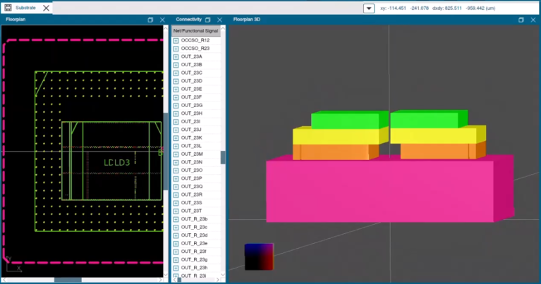
- 2D assumptions in a 3D world: Current physical verification tools rely on formats like GDSII, which infer vertical relationships. This breaks down completely when you have multiple dies stacked or placed side-by-side with complex routing, where geometries on the “same layer” might actually be vertically displaced.
- Inconsistent layer mapping: Chiplets come from various foundries, each with their own unique layer mapping conventions. What’s “metal1” at one foundry might be completely different at another, leading to misinterpretations and errors.
- Lack of true package-level LVS: Traditional Layout Versus Schematic (LVS) tools rely on SPICE-style netlists that go down to the transistor level. Package design tools don’t operate at this granularity, and SPICE is too bulky for package connectivity. This leaves a void in verifying electrical connectivity across the entire assembly.
- Increased risk and cost: Without formal, repeatable verification processes, designers are forced to rely on inconsistent methods, increasing the risk of costly re-spins, missed schedules, and even field failures.
The new class of advanced packages, like Fan-Out Wafer Level Packages (FOWLP), further blurs the lines between die and package, necessitating a unified co-design and verification flow.
Unlock advanced package verification
This blog post is just a glimpse into the critical challenges and solutions for integrating chiplets into advanced packaging platforms. The full story, including a detailed methodology and process, is available in our comprehensive eBook series by Keith Felton, IC Packaging product marketing manager.
(Source: Siemens)
Read more:
- Leonardo optimizes electronic systems with Xpedition, HyperLynx, and Valor
- Nobo Auto optimizes PCB design with Xpedition & HyperLynx
- Calibre Auto-Waivers