Products that run on software are integrated into our everyday lives. Smart devices and other software-defined products (SDP) are only due to become more common; as a response, organizations across industries are increasingly using software to enable the functionality of their products.
Along with increased demand, chip makers will have to contend with the high costs of creating chips. Already, building a fabrication facility (fab) to manufacture semiconductors costs around $19 billion and designing one costs another $1 billion. What’s more, each fab must be able to efficiently build chips in high volumes and very high yields to be able to ensure they work economically in the market. To meet the increased demand from consumers and companies alike, chip makers have begun to adapt to optimize their processes.
The emerging market
Gone are the days of saying: “let’s just get a processor and we’ll make it work with everything”. Instead of considering the platform and applications first, chip manufacturers now consider the purpose of the semiconductor-powered product. Many are now tailoring their processing platforms to specific products, taking into account the workload needed to handle it.
Customizing the semiconductor to the product has become even more vital as more products begin to increasingly rely on software. In the past, SDPs encompassed mainly personal devices such as computers and cell phones. These days, automakers and other heavy machinery manufacturers introduce essential software in their products that must function for their equipment to run safely. That’s why it’s absolutely critical that companies can develop platforms with customized processes in there tailored towards the workload the products to have to run from a software point of view.
Besides customization, the increased prevalence of AI is encouraging chip makers to take more innovative approaches to fabrication. AI chips consume a considerable amount of power, with some chips consuming as much as 1800 watts. Through deploying advanced packaging techniques, manufacturers can create more energy-efficient chips with the added benefit of reducing fabrication costs.
New design standards
With chips becoming more customized and complex, the design and production cycle will inevitably transform. Already, many manufacturers are seeing the already complex process of fabricating semiconductors become even more intricate.
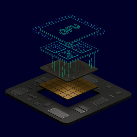
Before, it was not unusual for each team involved in the design process to work on the chip in parallel. Often, the semiconductor design team would receive a set of requirements to build the chip all while the verification team tested it, and this entire process was typically siloed. But now, the semiconductor device is becoming more complex, with a typical device moving from 15 billion transistors to 18 billion transistors.
As the scale of the design is increasing, the scale of the requirements and requirements management is equally exponentially increasing. The added complexity creates different domains of requirements which must be managed and more importantly, traceable and linked together, to ensure that each requirement is being built and tested.
Fabbing the future
SDPs and AI are becoming ubiquitous. The semiconductor industry is already adopting changes to keep up with demand. Companies are now moving away from standardized chips and moving towards chips tailored for specific functions; as well, to address the increased power consumption from AI chips, manufacturers are leveraging more advanced packaging techniques.
These changes increase the intricacy of the design and production processes, inspiring many organizations to beef up their requirements management platforms to increase traceability and improve communication between teams.
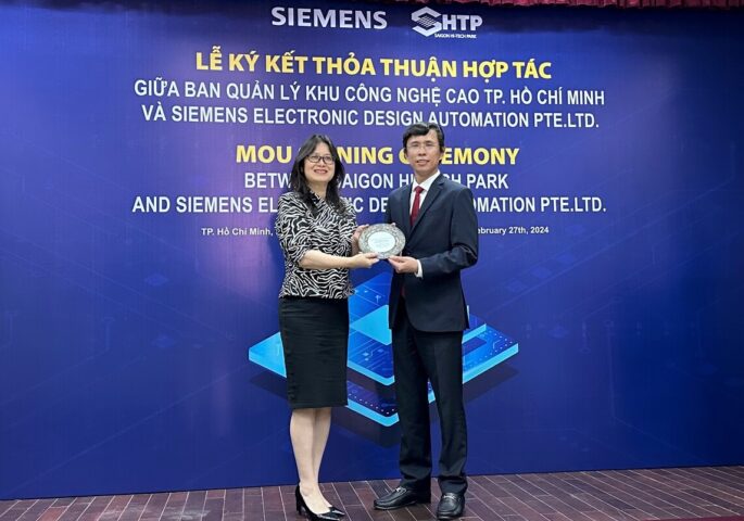
(Source: Siemens)
Read more:
- Arm finds success with Siemens Aprisa place-and-route
- Top 6 reasons to choose IC design solutions from Siemens EDA
Contact us for free and detailed advice