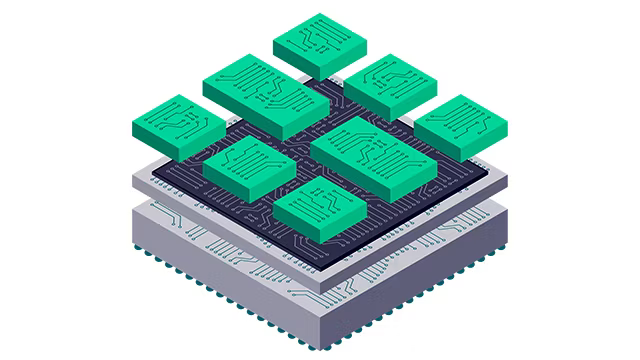
2D design is no longer sufficient for today’s complicated PCB layouts. Flex and rigid-flex designs, and an increasing need for collaboration with MCAD, require advanced 3D layout design capabilities to help fully address today’s challenges. For example, to ensure no physical violations occur when the PCB is placed within the enclosure or system, especially when designing with flex, the electrical and mechanical design must take component and mechanical clearances into account. There is no better way to do that than with advanced 3D layout.
By considering mechanical requirements during layout and ensuring efficient communication between the electrical and mechanical flows, the design is correctly aligned for manufacturing, avoiding last-minute changes that cost time and money.
With advanced 3D layout, the PCB designer can be more involved and have greater visibility over the mechanical aspect of the design, allowing him or her to place and route components while adhering to mechanical requirements. 3D design does not replace communication with MCAD engineers, but it improves and shortens the design cycle by reducing iterations.
This post describes six ways to maximize the benefits of 3D technology.
1. Use 3D layout for viewing, placement, and more
Advanced 3D layout allows immediate identification of critical areas in PCB designs, enabling engineers to resolve electro-mechanical problems on the fly. Catching problem areas early, during the design phase, eliminates costly, last-minute changes that otherwise might not be found until the mechanical CAD group finds them in the completed design or, worse, until manufacturing.
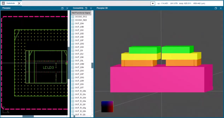
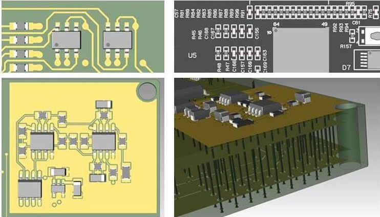
Designers often want to investigate internal layers to identify non-functional padstacks and internal plane layers. Being able to scale the thickness of the board and provide cuts in the X, Y, and Z directions (figure 1) will immediately highlight potential design issues.
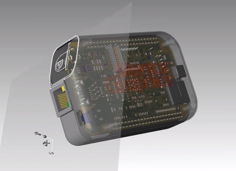
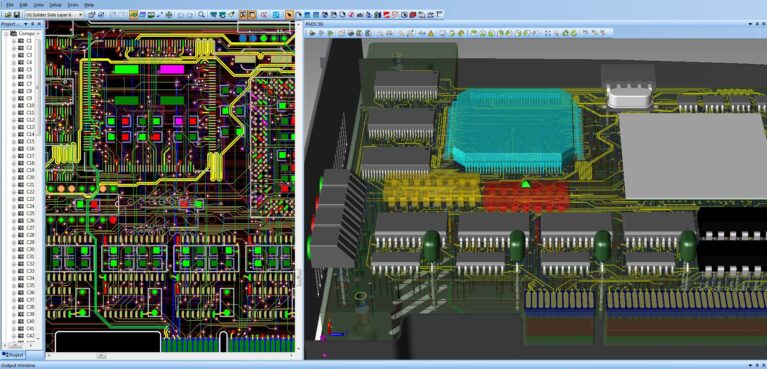
3D viewing is more than an interpretation of 2D information; it’s a true photorealistic view of how the design will be fabricated, that provides superior visualization of complicated structures. It’s extremely helpful to have controls, including transparency, for board elements such as traces, components, silkscreen, solder mask, and vias. Use the controls to visually find electromechanical conflicts that would be difficult to identify in a 2D view prior to running design rule checks from manufacturing.
With an integrated 3D view of the layout, designers and engineers can immediately validate PCB designs to identify over- and under-constrained areas in the design, thereby freeing up real estate and reducing potential electrical issues.
Placement strategies, available in some design tools, can help reduce board real estate and lower the layer count. A good way to investigate place- ment strategies is to use 3D placement groups.
Such groups allow the quick identification of the minimum X, Y, and Z real estate required when all components are placed.


2. Add 3D parts quickly and easily
3D starter libraries are great but, for 3D design, 3D components are also needed. Although 2D compo- nents can be easily created using wizards, creating 3D components and mechanical parts is a different story. It typically requires a mechanical engineer to draw the component in a system such as Creo® Parametric™ or SolidWorks® and add it to the parts library. This task requires CAD knowledge and tool licensing that are not always available to individual PCB designers or small teams.
An easy alternative is to import STEP models from vendors’ websites. After downloading and importing the STEP file, the downloaded part in the parts library needs to be mapped to make it available and easily accessible in future designs.
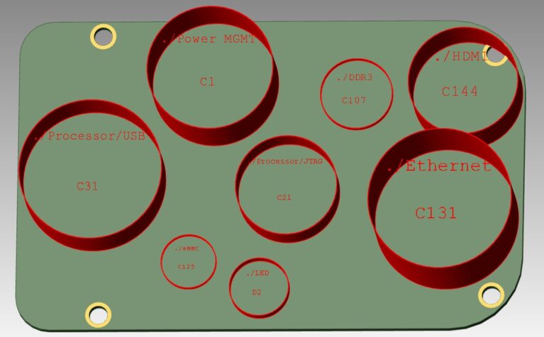
3. Set 3D constraints and clearances
For confidence in designing layouts according to the mechanical requirements, it’s extremely helpful to set 3D constraints in layout. To maximize work efficiency, define 3D constraints in the same envi- ronment used for the rest of the design constraints. Constraints can be set to standard objects such as board edge, land patterns, and mechanical objects. Specific component footprints can also be override.
Based on the defined 3D constraints, online DRC will provide graphical feedback to show any violations of the constraints during component placement. This, along with a batch DRC of the entire board, helps design with confidence and ensure design constraints are met at all times.
constraints during component placement.
4. Communicate with MCAD
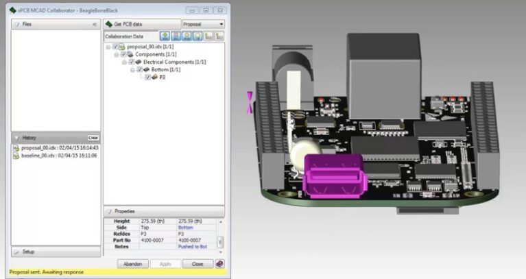
Communication and collaboration with MCAD is another area where having 3D layout abilities can make a big difference. There are two major chal- lenges when collaborating with MCAD: the actual communication format, and having the PCB adhere to mechanical demands as early as possible to avoid changes in later stages of the design cycle. A PCB design tool that solves both challenges can make a huge difference in the efficiency of the communica- tion with MCAD.
Let’s focus on the first challenge. Many companies still utilize Intermediate Data Format (IDF) to transfer information between electrical and mechanical systems. Using a static file transfer of an entire database makes it hard to identify changes and usually requires more documentation time.
Missing, or missed, design information increases the overall PCB design time.
An integrated ECAD/ MCAD collaboration tool allows both the designer and the MCAD engineer to be fully synchronized. Issues in communication can be identified easily and effective collaboration on critical design items across domains ensures the design intent is kept. The end result? Prototype reduction and more robust designs that get to market faster, and at lower cost.
The availability of integrated 3D viewing and editing during PCB design helps with the second challenge, allowing designers consider mechanical demands from the start. With these capabilities, the PCB is better prepared and requires fewer changes when it gets to the mechanical engineer. Communication with the mechanical engineer will be more effective and take less time.
5. Improve flex design with advanced 3D layout
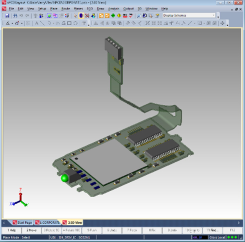
Flex design introduces a new set of difficulties for the PCB designer. Designing the stackup is more difficult, routing can be completely different, and even signaland power-integrity issues are more challenging. Advanced 3D, and the ability to measure in 3D where there are bent or folded assemblies, helps see whether a connector on a flex cable misses its target and, if so, by how much. Knowing this makes it easy to adjust the component placement or flex cable length.
Being able to export a 3D model of the bent Flex- Rigid assembly is also important, enabling the mechanical design team to import the PCB and use it in their 3D design environment.
6. Help manufacturers capture the design intent with 3D PDF
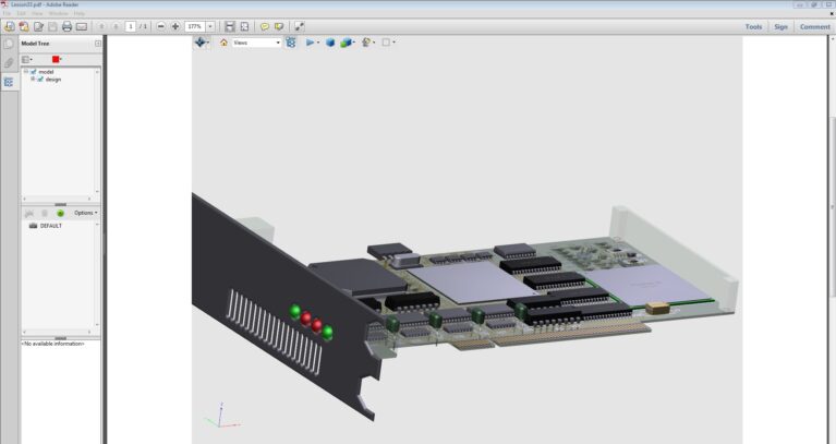
Before sending a finished layout to manufacturing, it can be beneficial to export a 3D PDF report of the design. Most tools have an option to export STEP as well but not everyone can open STEP files, so PDF is more approachable.
The 3D PDF report can be useful for reporting and documentation purposes but its primary purpose is to help manufacturers better understand the design intent and, in so doing, to properly manufacture the PCB. Many PCB designers testify that manufacturers have difficulty understanding what the PCB is supposed to look like based on a 2D report. Sharing 3D representations allows others to visualize the design and detect potential problems earlier.

Conclusion
Having advanced 3D layout capabilities can be highly beneficial when they are well integrated in the PCB design tool. Being able to view and under- stand information from the third dimension helps design better layouts from the start, both electroni- cally and mechanically. With 3D design, the designer has more control over design intent, better communication with mechanical engineers and, ultimately, higher-quality PCB designs.
Advanced 3D layout in Xpedition® provides the capability to visualize and validate PCB designs as if they were already manufactured. With Xpedition designers and engineers can easily understand the physical product, allowing identification of elec- tro-mechanical problems early in the design cycle and avoid costly re-designs. A complete photoreal- istic view of all board elements also helps with flex design challenges.
Xpedition also includes a 3D library of 4.8 million parts, allowing the validation of complex PCB designs with rigid mechanical constraints. The 3D layout environment supports real-time collaboration within the MCAD system, allowing ECAD/MCAD users to negotiate changes within the electrical
and mechanical domains.
For more information, please contact:
Vietbay CAD/CAM/CAE/PLM Team
Phone/Zalo/Whatsapp: 091 929 5520
Email: [email protected]
Website: www.vietbay.com.vn * www.cadcamcae.vn * www.vietbay.edu.vn