IC design, or IC manufacturing are very common phrases for engineers. However, very few people know and deeply understand its production process.
In this article Vietbay will guide you through the steps of designing and manufacturing ICs. Find out the information below!!!
1. Development history of IC
The development history of integrated circuits (IC) began to appear in the 1950s, starting with the first invention of the transistor by Bell Laboratories in 1947, which helped replace transistors. Large sizes were used earlier in electronic circuits, then electronic circuits were made by manufacturing discrete components and integrating them together. By 1958 Jack Kilby and Robert Noyce announced the implementation of electrical circuits on a semiconductor block called the first integrated circuit. And he won the Nobel Prize in 2000.
Over time, the development of electronic circuits has had an amazing explosive growth, from integrated circuits containing only a few dozen transistors called Small-Scale integration (1960) to integrated circuits containing millions or even are billions of Transistors called VLSI-Very Large-Scale integration (1980) or ULSI-Ultra Large-Scale integration ICs and these are also names commonly used today.

2. IC types
There are 2 main types of ICs commonly used today including Analog ICs (analog ICs also known as linear ICs) and Digital ICs (Digital ICs). For Analog IC both input and output signals are continuous. The output signal level depends on the input signal level, and the output signal level is a linear function of the input signal level. Linear ICs or analog ICs are most commonly used as audio frequency amplifiers and radio frequency amplifiers. Op amps, voltage regulators, comparators and timers are also good examples of linear ICs or analog ICs.
Digital ICs are integrated circuits that work with output signals in the form of binary numbers 0 and 1. Logic gates such as AND gates, OR gates, NAND gates, XOR gates, flip-flops, counters; Microprocessors are some typical examples of digital ICs.
3. IC design process
Normally the IC design and IC manufacturing process is carried out by the following steps corresponding to the Front-End and Back-End, manufacturing and testing and packaging stages.

Architectural design
First, designers need to build ideas and define the functions of ICs. ICs are designed in the form of hardware description language (Hardware description langue-HDL). At this stage, ICs are defined. definition in the form of block diagrams, combining hardware description languages to design functional diagrams of ICs, commonly used hardware description languages such as Verilog or System Verilog, analysis tools Evaluation is also performed at this stage to ensure the IC functions properly, this stage is also called RTL (Register transfer level) design. There are many different software that support the architectural design phase such as Catapult HLS or 3D IC software from Siemens EDA (Mentor Graphic).
Logic design and Verification
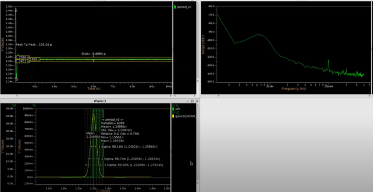
After completing the functional diagram design, the design is carried out to describe the connection through logic gates. At this stage, the components are connected. In this step the macro-level building blocks are assembled and connected together to perform the necessary function of the IC. Typically, off-the-shelf building blocks are used, such as memory, processors, and sensors. The high-level functional descriptions of the circuit elements are decomposed into the necessary low-level circuit elements. This process is automated using software called logic synthesis (Synthesis). A collection of devices are simulated to verify the functionality of the design. Either a digital logic simulator or an analog circuit simulator will be used, depending on the level of simulation detail required. If macro-level building blocks need to be modified to achieve IC requirements, custom circuit design techniques are used. In this step, the “how” of chip implementation begins to be determined.
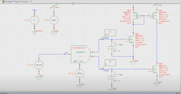
Can use software such as Questa, Power pro, Tessent to design IC logic diagrams and use AFS, Questa, Sympony, modelsim… To simulate IC analysis
Physical Design
In this step, the actual layout of interconnected shapes implementing all the necessary circuit elements on the silicon wafer will be created. This process starts with a “Floor Plan” of the chip. In this step, the components and component clusters of the IC will be arranged on a specific semiconductor substrate, determining the location of each function. main chip and the location of the main input and output ports of the design, next is the placement step. In this step, you need to arrange the location of the logic connection ports in the most optimal way, Then, the final circuit elements are routed together in preparation for the manufacturing process.
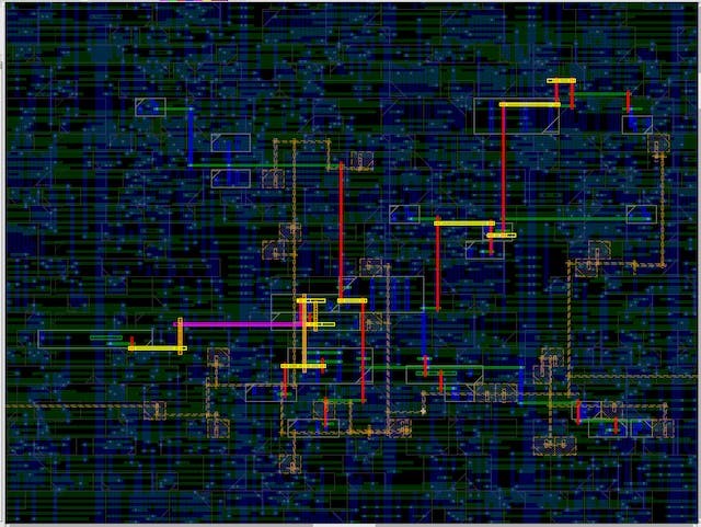
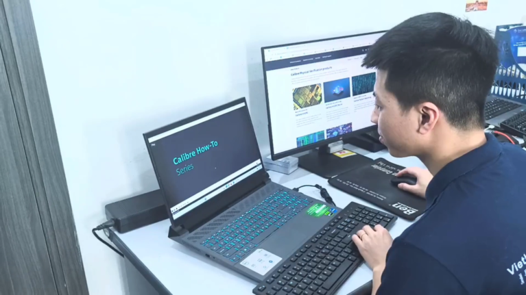
There are many different Siemens EDA software tools that support the physical design process such as Aprisa, Caliber, Tanner, Precision.
Physical Verification
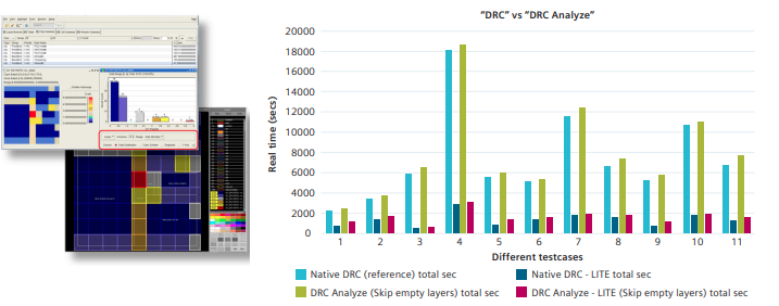
Influential factors related to the manufacturing process and factors affecting the working efficiency of the IC are considered and considered in this step such as resistance, radial noise, electrical rules… to ensure that the IC can work well in real conditions after production. At the same time, checking factors affecting production to ensure that IC designs can be manufactured after being designed (DFM) must also be calculated and analyzed in this step. After being analyzed and evaluated, the step of creating masks and film rolls can be carried out. The films will be sent to the manufacturing plant to create ICs on semiconductor substrates. These films will be made on the roll of magnetic tape. Software supporting Siemens EDA’s physical verification process such as Calibre, Tessent, mPower
IC manufacturing
After completing the design, the design data is exported in the form of a magnetic roll containing images and other related information. The data is transferred to the production process through many stages, including: includes the main steps of creating chip cores on the wafer and then the chip cores are cut separately, each chip core is created in a shell to become a finished chip (IC Packaging).

Refer to the following IC design software:
Contact us for free and detailed advice: