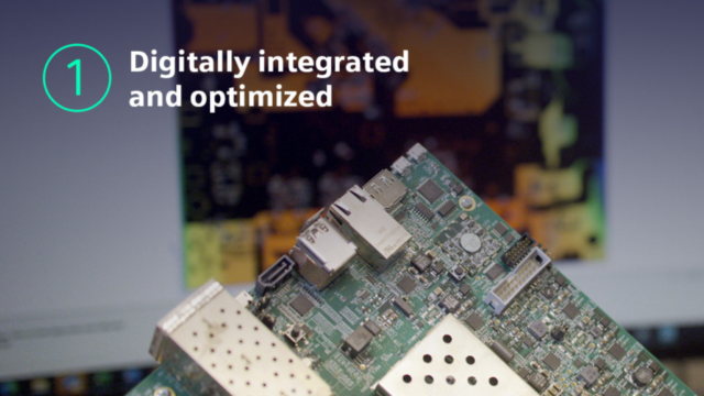
DFM is critical for the challenges of manufacturing flex circuit designs.
The use of flexible printed circuit boards (PCBs), whether stand-alone or to connect rigid boards, has rapidly grown over the past decade. This growth has been driven by the proliferation of smaller form factors of products, such as wearable electronic devices. Because of their unique properties, flex circuits require special manufacturing methods compared to rigid PCBs and can be less tolerant of issues that negatively affect manufacturability.
Barriers to shifting DFM to design
Flex circuit designs have unique properties and materials that separate them from rigid printed circuit boards (PCBs) (Figure 1). The flex circuit’s thinness makes them more delicate, and they are more susceptible to accidental damage during manufacturing. This negatively affects the yield, increasing the per-item cost.
Figure 1. Flexible circuits introduce new challenges compared to rigid PCBs such as bending and flexing as well as different adhesion characteristics of copper traces.
Flexible circuits are typically built using a combination of material types and methods. These various materials present a challenge for manufacturing. When combined with typical FR4 PCB materials, the complexity increases. The greatest challenge is posed by differences in the thermal expansion characteristics of the various materials. These characteristics need to be addressed in DFM reviews.
Ten challenges that make flex and rigidflex circuits more difficult to Manufacture
Flex circuits and the interface between rigid and flex segments can have problems that do not exist with standard rigid PCBs. The following are some potential problems and how to solve them proactively.
SMT components on the flex material
Placing surface-mount components on the flex circuit is possible by using selectively bonded stiffeners where required. Copper on a flexible substrate is more susceptible to delamination than a typical rigid board; consequently, surface mount pads require support, typically using a coverlay overlap onto pads and vias. Enlarged pads can be used instead of a coverlay, which provides greater area on the pad to adhere to the laminate. Using both support methods produces a pad with excellent adhesion.
Make pads larger than holes in coverlay
Making pads larger than the access holes in the coverlay can significantly increase bond strength while decreasing delamination possibility. This technique is similar to solder-mask-defined pads for rigid PCBs. With flex designs, the coverlay adds additional anchoring to the copper features.
Bend area conductor spacing
Bend areas are another area for careful design. The rule-of-thumb for conductor spacing is 5 mm between the rigid board and the bend area of the flex circuit (Figure 2). Bends closer than this are much more susceptible to breakage. Also, without proper spacing, the coverlay under the rigid area can peel and expose copper.
Sharp trace angles at bend points
There is a second issue with bend areas relating to trace direction. Flex-circuit reliability and quality can be improved by ensuring that traces flow into the flexible circuit bend with little or no change in trace direction, also seen in Figure 2. If a change must be made in the direction of the traces in the bend, use curves instead of angled paths to reduce the chance of cracking the traces in the bend.
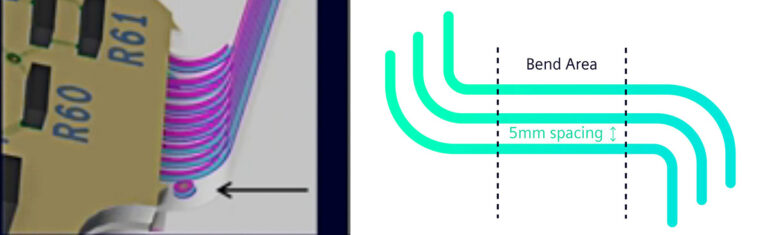
Figure 2. Conductor spacing should be 5 mm between the rigid PCB and bend. Also, traces should not change direction within the bend area.
Conductor width
Conductor width is also especially important. A safe rule-of-thumb for conductor-widths is to design them at least five times as wide as they are thick. Our recommended practice is use the thinnest copper trace that will safely carry the intended signal and then adjust trace width accordingly.
Plane hatching
Stress at the bend points can be relieved using a technique called plane hatching. While a honeycomb shape (hexagon) will alleviate the most angular stresses, any hatching will have a strain reduction when compared with that of a solid shape.
Pad fillets improve strength
Pad fillets, shown in Figure 3f, improve the yield and strength of flexible PCBs. They should be employed in instances where the diameter of the pad exceeds the connecting trace width. You should also avoid acute angles at the interface between traces and pads with fillets to minimize the stress at the junction.
Interface region
Typically, the area extends about 1.2 mm from the edge of the rigid board and into the flex area for a combined 2.5-mm region. The interface region can be more fragile than the rest of the design, requiring special design considerations. These include avoiding vias, mounting holes, slots, plated through-holes close to where flex and rigid join and designing the angle where traces enter rigid sections of the circuit to be anything other than 90 degrees.
Relaxed tolerance
Tolerances for flexible circuits must be more relaxed than for rigid PCBs. The materials and construction techniques used in flex circuits can shrink, expand, stretch and compress in different ways than rigid PCB counterparts. Relaxing tolerances allows for these events.
Thermal expansion
Most adhesive-based flex base materials are unfilled, which may result in unchecked thermal z-axis expansion, which makes vias and other features prone to delamination and causes potential intermittent responses after components have been soldered to the surface of the flex material. To combat this, include a more robust pad stack compared to the rigid areas for components soldered on the flex material.
Your flex DFM solution: Valor NPI
Flex and rigid-flex circuit designs are increasingly popular with the miniaturization of technology and the explosion of wearable devices. PCBs involving flexible circuitry require unique manufacturing processes. To ensure and optimize flex and rigid-flex circuits for manufacturing, a dedicated DFM solution combined with an intelligent, comprehensive manufacturing product model are the best combination of tools to improve the yield, cost and reliability for flexible circuit designs.
Valor NPI is such a solution that brings the manufacturing knowledge into the application to provide the expertise to run DFM on PCB designs. Valor NPI provides complete DFM coverage for both rigid and flexible circuit boards as well as the interfaces between them.
Valor NPI can identify issues associated with the 10 challenges presented here and many others. Identifying and rectifying issues early on can save time, money and, best of all, redesigns because of manufacturing issues. Flex circuitry is more difficult to manufacture than rigid PCBs, and the best way to ensure that designs are manufacturable is to run DFM checks throughout the layout process as well as running DFM on the manufacturing release process.
Running DFM checks on PCBs with Valor NPI can reduce respins on average by 57%. For rigid/flex, it is even more critical to ensure manufacturability before sending the product model data to the fabricator. Applying DFM to PCB designs results in more time spent designing and less time fixing.
Contact us for free and detailed advice