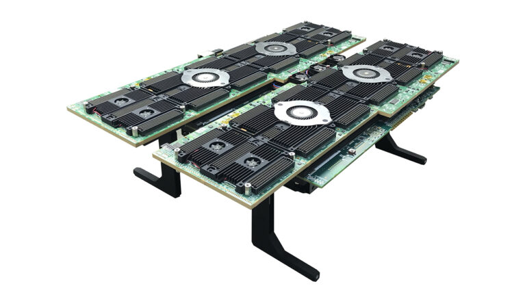
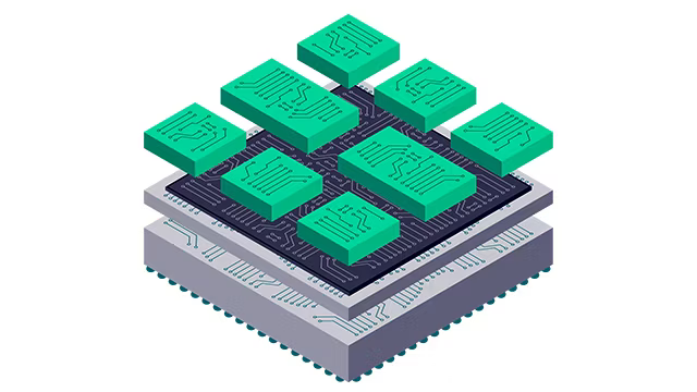
Semiconductor engineers aim to deliver best-in-class devices despite technology scaling and cost limitations of monolithic integrated circuit (IC) design. To overcome these challenges, teams turn to heterogeneous integration and the 3D stacking of ICs and specialized chiplets.
3D IC enables companies to partition a design and integrate silicon IP at the most appropriate process node and process, providing lower manufacturing costs, higher wafer yields, lower power consumption and lower overall costs.

Benefits of chiplets for 3D IC design
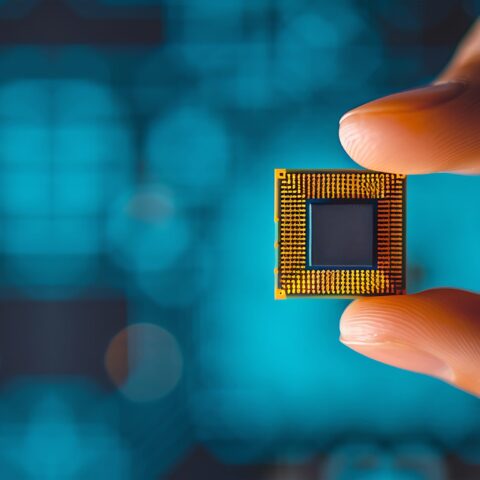
Designers can use chiplets to meet or exceed PPA goals with 3D IC while improving differentiation, profitability and time-to-market. Chiplets are small ICs specifically designed and optimized for operation within a package in conjunction with other chiplets and full-sized ICs.
In heterogeneous designs, chips and chiplets are stacked and interconnected with vertical wiring. Designers can also combine them with 3D memory stacks, such as high bandwidth memory, on a silicon interposer within the package of a device.
3D IC and the system technology co-optimization (STCO) approach
Companies wanting to pursue heterogenous integrated design must adopt four enabling approaches:
- Transition from design-based to systems-based optimization for consistent system representation throughout design
- Expanding the supply chain and tool ecosystem requiring interoperability and openness
- Balancing design resources across multiple domains with system co-optimization (STCO)
- Globalization requires complete system focus and cohesiveness across engineering teams (silicon, packaging and PCB) around the world
3D IC workflows packed with powerful capabilities
The Siemens heterogeneous 3D IC solution enables teams to create designs that meet or exceed PPA goals and improve the differentiation, profitability and time to market.
- Heterogeneous planning and co-design using prototyping/planning and integration of 3D IC packages enable a full system perspective for STCO-based modeling and early prototyping
- Ecosystem interoperability and openness with industry standards, supporting third-party tools, certified reference flows, process design kits (PDK) and assembly design kits (ADK)
- Physical verification through industry-proven assembly-level 3D IC verification (DRC/LVS)
- Multi-domain testing for 3D IC architectures with known coverage through standards for 3D IC multi-domain testing
Caliber IC design solution in IC verification
Caliber IC design solutions are the industry leader in IC verification, providing a complete IC verification EDA platform and DFM optimization that accelerates designs from creation to manufacturing, addressing all request sign-off.
Top 5 IC Caliber design solutions:
- Caliber physically verified
- Caliber verifies the circuit
- Caliber verifies reliability
- Caliber designed for production
- Caliber interface
Learn product details right here
Source: siemens
| Vietbay – authorized partner of Siemens EDA on IC&PCB design solutions for customers in the Vietnamese market. |
Contact us for free and detailed advice