As consumer electronic devices grow increasingly connected, intelligent and advanced, designers need new methodologies such as 3D IC to address more than Moore limitations. The increasingly complex devices include more features and more complex electronic circuit design, requiring more processing capability. To keep up with these demands, designers need new methodologies for designing and connecting chips.
Join Vietbay to find out the details below!
Watch the 3D IC podcast episode: An Introduction to 3D IC
If you prefer video to text, watch this 22-minute introductory video about 3D IC. Learn the basics of 3D IC advanced packaging, current trends and challenges for adoption.
We know that everyone has their own preferred learning style, and we want to make sure you can get the most out of this content in the way that works best for you. So, whether you prefer to read the copy below or watch the full episode above, we hope you find this information helpful!
What is 3D IC?
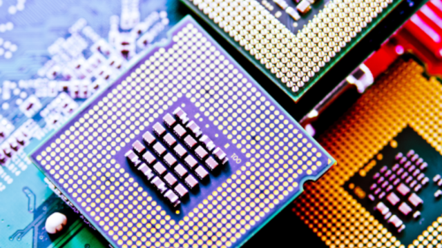
3D IC is a three-dimensional integrated circuit and refers to the integration, methodology and technology. Design teams disaggregate traditional monolithic implementation architectures into several smaller functional chips or chiplets integrated using a high-performance package. These 3D integrated circuits take up less space and deliver much higher performance than traditional monolithic technologies.
Technology for high bandwidth memories (HBM) came out about ten years ago where multiple memory chips are stacked. These stacked chips provided a lot of memory for a small footprint and integrated into ASIC on a 2.5D interposer, which is where that term originated.
What problem does 3D IC solve?
The semiconductor industry saw advanced application-specific integrated circuit (ASIC) technology nodes scale dramatically over the last 40 years, alongside higher performance. As we reach the limits of Moore’s law, device scaling becomes a challenge. Devices shrink at a slower rate, it takes longer and the cost is much higher for the technologies, design, analysis and manufacturing of these chips.
There are practical limitations on how large you can make a device. The photomask and reticle size ultimately determine a chip’s maximum size – roughly 25 to 27 millimeters on a side. So, physically, you cannot make a chip bigger than that. Since the number of transistors scaling has reduced, designers do not benefit from increased complexity by putting more and more devices into a single package. 3D IC designers do not face the same footprint challenges.
System on a chip (SOC) intellectual property are the basic building blocks implemented in that chip. Different types of functions require very specialized ASIC technologies. In some cases, it could limit what you can implement in the system because you would need all the IP available in the same process if you’re going to integrate that into a single chip. When we get into 3D IC, you no longer have that limitation. So, you can acquire chiplets, which perform a particular function, such as intellectual property. That chiplet can be optimized using the most appropriate technology for that type of functionality.
How does 3D IC work?
Since 3D IC is not limited to how large a device can be, designers can create much larger systems by putting multiple chips in a package. The implications of monolithic design for high-performance computing and AI devices will continue to use monolithic technologies. But they could leverage some of this disaggregation by splitting the design up into a smaller set of chips. But in general, if you can fit everything you need in a single chip, you will get the lowest unit cost and the highest performance. When designers start facing limitations, that’s where 2.5D or 3D technologies can extend their capabilities.
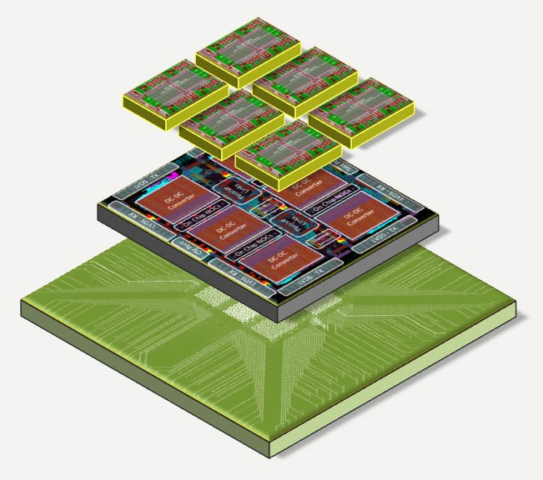
For years, designers created multi-chip modules (MCMs). They put one or more ASIC chips into a single package and connect them with traditional packaging technologies. MCMs are a very mature technology but also have some limitations. 3D IC is driven more by advanced packaging technology to integrate chiplets. A chiplet is an ASIC designed to integrate with other chiplets within a package. These chiplets come in two classes:
- 2D (or 2.5D): Integrating two chips on a single interposer and interconnecting those chiplets on that interposer using metal interconnect.
- 3D: Die stacking involves stacking memory or sensor chips on another chip (like memory). True 3D is a very advanced technology that splits an ASIC into two chips and stacks them.
None of the available choices semiconductor design teams have to counter some of the monolithic challenges seem to be a “one size fits all” or complete solution.
What’s different about 3D IC from other technologies?
The difference between the traditional MCM is the packaging technology – so that may be either 2D or 3D. One key difference is the interconnection between devices at the silicon level. The wires are much shorter and thinner, making the resistance and capacitance considerably slower and allowing for more connections between chips.
In effect, 3D or 2D packaging technologies enable increased performance with greater complexity with more interconnects – allowing designers to build systems with a much smaller footprint inside of a single package.
Designers can decompose systems into functions implemented as smaller chips, or chiplets, instead of putting everything into a single homogeneous ASIC device.
The other difference here is system designers now have more options to implement their complex devices and take advantage of some of the inherent benefits of 2.5D and 3D. So it offers them more options in developing their systems, taking advantage of some of the benefits provided by these technologies.
What challenges do we face with 3D IC?
Now that we know what 3D IC integration is and how it’s different from other advanced integration packaging technologies, we know there are some challenges in moving into 3D IC:
Thermal management
A traditional ASIC device uses a very simplified single power profile. In 3D IC package, designers must manage the thermal power profiles of multiple chips. Designers also need to understand the thermal interaction between different components to ensure the package meets the thermal requirements of the device.
Mechanical stress analysis
When you stack die or stack a large silicon interposer on top of an organic substrate, the thermal expansion coefficients between the materials are different, so they will bend and flex differently. The potential mechanical stress on the connections between those devices can cause failures and reliability issues. Since every design is unique, designers should perform analysis with mechanical simulators to model that stress.
Designing and analyzing the power delivery network
Package designers must consider that multiple chiplets may have different voltage supplies, power and noise requirements.
Testability
Likely the most complex issue for 3D IC is testing, which is typically is a two-step process for single devices. The two types of testing are wafer-level and final testing once the chip is in the package. There are multiple chips inside 2.5D and 3D devices. Manufacturers likely wafer-tested them before delivery to the system integrators but would still require testing the interfaces between chips and restest packaged devices.
Caliber IC design solution in IC verification
Caliber IC design solutions are the industry leader in IC verification, providing a complete IC verification EDA platform and DFM optimization that accelerates designs from creation to manufacturing, addressing all request sign-off.
Top 5 IC Caliber design solutions:
- Caliber physically verified
- Caliber verifies the circuit
- Caliber verifies reliability
- Caliber designed for production
- Caliber interface
Learn product details right here
Source: Siemens
| Vietbay – authorized partner of Siemens EDA on IC&PCB design solutions for customers in the Vietnamese market. |
Contact us for free and detailed advice