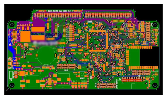
The demand for electronics with gigahertz wireless technology, as well as IoT consumer devices have both increased dramatically. This has resulted in the subsequent increase of RF circuitry on designs. Therefore, the keyword “RF design” is also searched more.
Let’s find out useful information with Vietbay below!

The unique design requirements of RF designs
An engineer recently told me that their design only had about 10% RF circuitry on it, but that 10% takes up 90% of their design time to complete! This is because RF designs often have unique design requirements. These requirements typically can include very specific trace and via geometries such as:
- Tapered traces
- Traces with chamfered corners or arcs
- Co-planar wave guides
- RF components built to exacting dimensions out of metal

Regulatory certification and oversights
In almost all cases, these electronic products (electronics with gigahertz wireless technology, as well as IoT consumer devices) typically need to comply with regulatory certification and oversights. This may lead to failed compliance testing in an FCC or CE lab. A failed test means lost time – the product will require some type of an engineering change, redesign, manufacturing of the product again, then back to testing.
RF specific automation in your PCB design tool
RF designers need access to PCB design tools that have the features and functionality necessary to efficiently design to the unique requirements of RF. This means going beyond just manually drawing the unique geometries. Since these RF components, traces, and vias need to be created to exacting dimensions, RF specific automation needs to be available to create them correctly, and quickly.

RF simulators
Many RF engineers rely on RF simulators and other tools to help them with their designs. A very popular simulator is ADS from Keysight. The ability to directly import intelligent RF objects from ADS into the schematic and PCB design tool, or export to ADS is a must have feature. The alternative is to build the RF element manually, which is not only time consuming, but also error prone.
There are many other niche RF simulators that focus on specific RF components: filters, couplers, antennas, etc. A common output of these is DXF. The ability for the schematic or PCB tool to import these DXF files, convert them to an intelligent RF component, with the ability to store in the library for future use, is essential.
Find the right PCB design tool
To successfully design with RF circuitry accurately and within your design time schedule, be sure your PCB design solution has the automation to create the RF elements to your exacting requirements and integrate with the RF simulators that you use.
To learn more about RF design with PADS Professional Premium: https://vietbay.com.vn/en/?s=PADS
Contact us for free and detailed advice:


