The Gerber data transfer format has been serving the PCB manufacturing industry for decades, and the Extended Gerber standard (also known as RS-274-X) has been the most widely-used format in the industry since it was introduced back in 1998. It is commonly accepted in industry circles that Gerber is the most trusted and reliable format.
However, it is clear to all that Gerber represents “the lowest common denominator”, and that it does not contain much of the data that is critical for manufacturing. Yet the common belief is that “manufacturers can manage” with Gerbers when accompanied by auxiliary data… because they have managed for decades.
Indeed, manufacturers can manage. In many cases, however, this means that the data that is stripped away when a PCB design is exported to Gerber must be “reverse-engineered”. In this post, Vietbay try to shed some light on what this takes from a manufacturer’s point of view.
Gerbers have arrived. What now?
First things first. Usually Gerbers arrive in a zip archive that contains lots of files:
- Each board layer is a separate file
- Every auxiliary layer (such as a drill map or a manufacturer drawing) is also provided as a separate file
- Every drill layer is also in a file – usually in Excellon format
- Miscellaneous documentation, in text, doc, excel, pdf, dxf, jpg, and other formats, is also part of the package
So how do you distinguish between all these files? In the best case – files will be named according to a naming convention that a human can understand, so the person who receives the package will be able to find relevant information reasonably quickly. Another helpful approach is the inclusion of an additional document that contains a textual description of each file’s role, hopefully in a language that you can read. But getting all this helpful information is more a matter of luck – as it has nothing to do with the format.
And if you are less lucky, you’ll need to open each and every file using a Gerber viewer or CAM software, and then try to understand the role of each file based on the graphic information provided (after all, each file is nothing more than a two-dimensional picture). Then, this information is entered into the CAM system by layer, including:
- Layer role
- Position in the layer stack
- Polarity – in case of negative power-ground layers
- Span – in case of partial drill layers
- Other attributes required for further processing of the board before production
So the layers are ready. All good?
Tens of different Electronic Design Automation (EDA) systems feature tens of different ways to create Gerber files. When multiplied by the tens of different CAM systems that have tens of different ways to read the Gerber files, this results in hundreds of ways that the graphical data can be interpreted. Indeed, in 95% of the cases, the interpretation is correct. But in the remaining 5%, the misinterpretation might be disastrous. Manufacturers that wish to leave no chance for misinterpretation will spend additional efforts reviewing the graphical data using various tools – to make sure that the data looks good. One of the best ways to check data integrity is netlist verification – a process of comparison between the netlist supplied with the Gerber package and the one calculated from the actual data. However, since netlist data is not part of the Gerber format – it may or may not be provided alongside Gerber files. Many manufacturers say that approximately 50% of design packages are supplied without a netlist. So if no netlist is provided, the second best method for verifying data integrity is visual. Sounds like something you should trust?
Ok, the data looks good. Can we proceed?
The data has been verified graphically. But what about its functionality? When designing a board using an EDA system, the layout engineer understands the functional role of all graphic elements on the board. For example:
- Pad role: surface mounting, BGA, via, etc.
- Drill types: plated, non-plated, mechanical via, laser via, etc.
- Trace types: impedance controlled traces, legend/nomenclature lines, tie bars, etc.
However, all this information is literally being lost in translation, since the Gerber format does include meta-data on graphical elements. All this data needs to be restored by the manufacturer either by manual information retrieval from documentation or by using sophisticated CAM tools – and in most cases, a combination of the two is needed to accomplish the job.
One more aspect that has to be manually recovered is information related to the Z-axis. In my previous blog post, “PCB Aspect Ratio – how do you know your board is manufacturable?”, I presented an example of aspect ratio calculation, which requires knowledge of thickness values. There are many cases in which the manufacturer needs to know the total board thickness, the copper thickness for each layer, and other values that are known in the EDA system but get lost in the Gerbers.
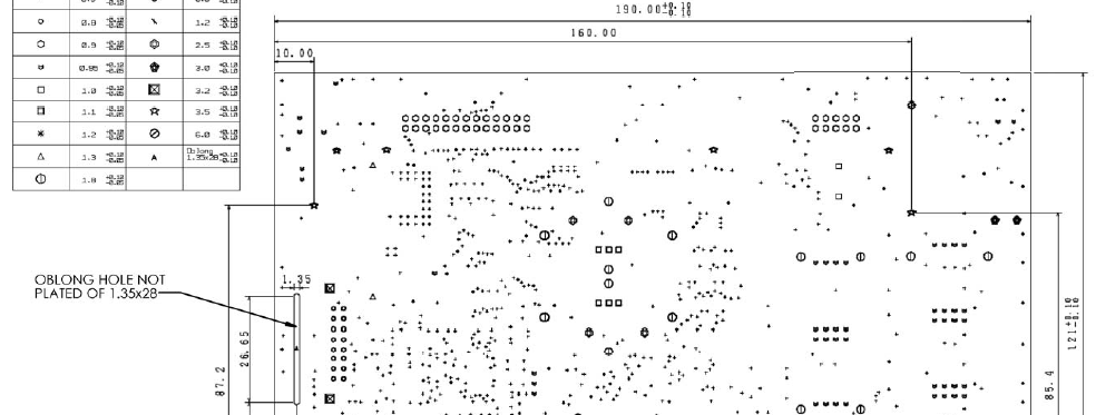
And here’s my favorite – the board outline, also known as the board profile. Here, also, the manufacturer depends on luck – it might be delivered as a separate auxiliary layer or implicitly drawn in other layers. But if not, it must be manually re-drawn, based on the documentation. In extreme cases, professional CAD skills are required, as board profiles may be highly complex, as in case of rigid-flex boards.
ODB++ and PCBflow
ODB++Design (formerly known as ODB++) is a comprehensive PCB manufacturing data format. Unlike the Gerber format, which requires multiple files and lengthy reverse-engineering by manufacturers, ODB++Design generates a single folder containing all the data necessary to fabricate and assemble PCBs.
ODB++Design contains everything needed to make sure there is little to no chance left to human or machine error during the design-to-manufacturing handover. It is field-proven for over 20 years and it is supported by all of today’s EDA solutions – and thus it should be the format of choice for your design-to-manufacturing handover to assure its accuracy, safety and efficiency.
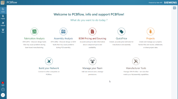
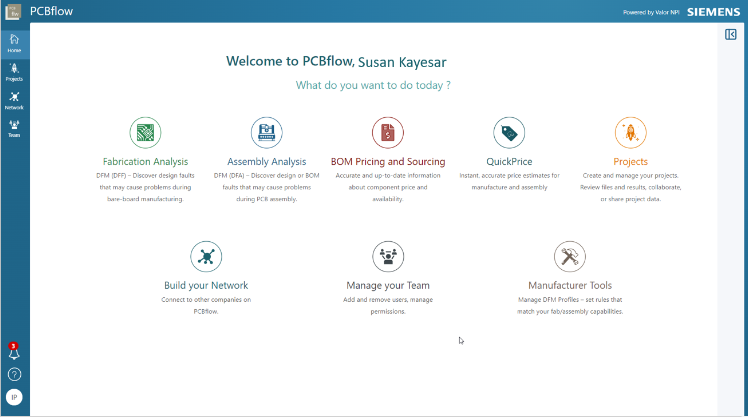
PCBflow is an online Design-for-Manufacturing tool and collaboration space for PCB designers and manufacturers. PCBflow leverages the completeness of ODB++Design, making the handover process virtually seamless — by enabling instant analysis of PCB layouts against a specific manufacturer’s production constraints.
Source: Siemens
Contact us for free and detailed advice

