
As artificial intelligence (AI) and high-performance computing (HPC) systems demand increasingly massive data bandwidth, the physical limitations of monolithic chips have driven the semiconductor industry toward advanced packaging technologies.
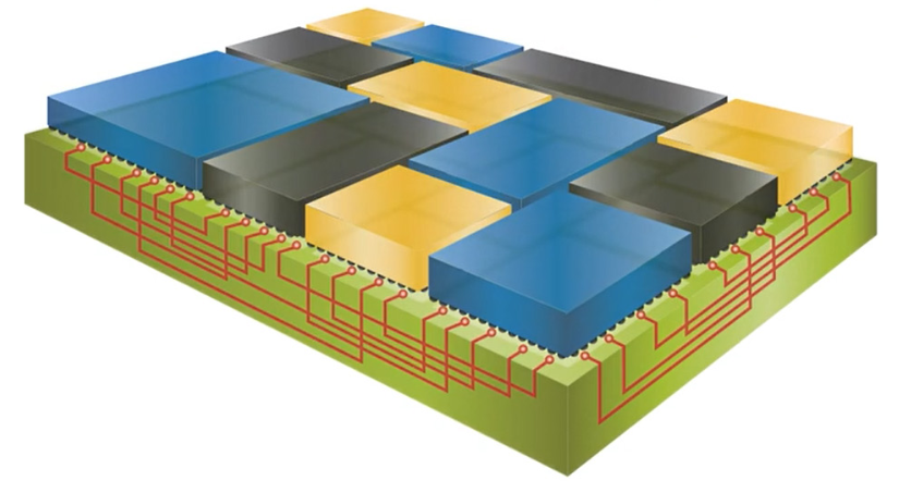
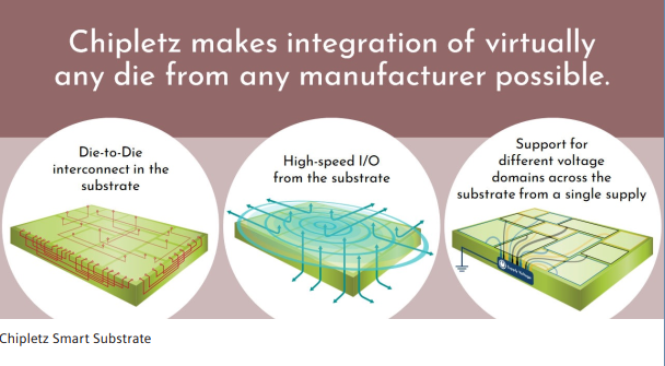
Recognizing this trend, Texas-based startup Chipletz has developed the Smart Substrate platform, a solution that enables multiple silicon dies manufactured using different process technologies to be integrated into a single package.
However, the complexity of this architecture introduces significant technical and financial risks. To mitigate these risks, Chipletz has standardized its entire R&D workflow using licensed software solutions from the Siemens EDA ecosystem, with a particular focus on HyperLynx.
Technical Challenges and Financial Risks
Smart Substrate aims to optimize performance through high-speed interconnects between dies and support for high-bandwidth memory (HBM) interfaces.
To achieve this, the physical design must meet extremely stringent requirements, including:
- Managing thousands of internal interconnect nets.
- Handling the power distribution network (PDN) across multiple voltage domains.
- Suppressing crosstalk in densely packed layouts.
From a business perspective, these challenges create two major risks:
- Rework costs: If signal integrity (SI) or power integrity (PI) issues go undetected during simulation, the company may need to manufacture a new mask set at the foundry. Each design correction cycle can cost millions of dollars and delay product launches by three to six months
- Engineering team productivity: A fragmented design environment or a lack of detailed parameter analysis forces R&D teams to rely on experience-based assumptions rather than accurate data, reducing overall productivity.
Smart Substrate designs impose requirements that push beyond the conventional capabilities of both engineers and EDA software. Whether a tool can handle these boundary-case challenges is a decisive criterion for us.
According to Michael Su, CTO of Chipletz
Solution from Siemens
To mitigate these risks, Chipletz evaluated multiple EDA platforms before selecting Siemens’ licensed semiconductor package design technologies, including:
- Xpedition Substrate Integrator
- Xpedition Package Designer
- HyperLynx
Within this ecosystem, HyperLynx plays a central role in analyzing and verifying signal and power performance for complex package designs.
Licensed software provides Chipletz engineers with advanced simulation tools to:
- Perform signal integrity analysis on high-speed data channels.
- Evaluate power integrity across power distribution networks.
- Detect and mitigate crosstalk between signal traces.
- Optimize the topology and routing of high-speed interconnects.
- Verify designs before moving into manufacturing
With its accurate simulation capabilities and high processing performance, HyperLynx enables engineers to work confidently with large-scale, highly confidential designs while maintaining efficiency throughout product development.
Implementation in a Large-Scale Project
To evaluate the practical capabilities of Siemens tools, Chipletz developed a highly complex test prototype based on its Smart Substrate technology.
The design included:
- One large-scale SoC.
- Four HBM memory stacks.
- Decoupling capacitors integrated into the substrate.
- A package measuring approximately 50 mm × 65 mm.
The complexity of the design is reflected in the following specifications:
- More than 8,000 interconnect nets between dies.
- Approximately 1.2 million vias.
- More than 180,000 component pins.
- A BGA with 2,800 balls.
In such a densely packed design environment, ensuring signal performance and power distribution integrity is essential.
HyperLynx was used to analyze high-speed signal channels and verify the power distribution system, enabling Chipletz engineers to proactively identify and address potential issues early in the design process.
As a result, engineers could optimize interconnect structures between chips and ensure system stability before moving into fabrication.
Read more:
- Optimize PCB Design with Xpedition Token and HyperLynx SI Analysis
- HyperLynx: Building Simulation Workflows for Electronic and PCB Design
Results: Architectural Breakthroughs and Cost Optimization
By adopting Siemens design and simulation technologies, Chipletz achieved positive results in both technical performance and financial efficiency.
The project successfully completed the design and tape-out of a test prototype based on the Smart Substrate platform.
In addition, Siemens tools helped significantly optimize the package architecture, delivering direct financial benefits:
- Reduced metal layers from 16 to 9: Significantly lowered material and fabrication costs.
- Improved design efficiency and system performance: Through secure and legitimate design IP reuse, Chipletz substantially enhanced its design workflow efficiency and overall system performance.
According to Bryan Black, CEO of Chipletz: “By enabling secure and legitimate reuse of design IP, Chipletz has significantly improved design workflow efficiency and overall system performance.”
The Role of HyperLynx in Next-Generation Semiconductor Design
In modern semiconductor systems, particularly multi-die and chiplet architectures, having the right tools to ensure signal and power integrity is critical to achieving optimal system performance.
HyperLynx helps engineers:
- Analyze and optimize signal integrity for high-speed interfaces.
- Ensure power integrity across power distribution networks.
- Detect and resolve design issues early.
- Verify designs before manufacturing.
With its ability to handle large-scale, highly complex designs, HyperLynx has become an important tool for developing advanced semiconductor systems for AI, HPC, and next-generation electronic applications, helping improve engineering efficiency and reduce costly design iterations.
Vietbay – Siemens EDA Solutions Partner in Vietnam.
Contact Vietbay for direct consultation tailored to your design requirements.